
Toshiba TK100E10N1| N-Channel Power MOSFET – 100V, 207A, TO-220
Out of stock
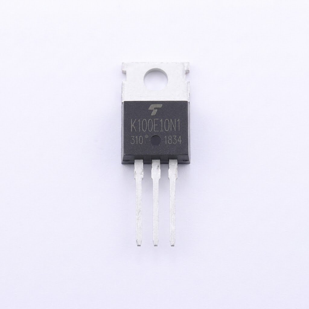
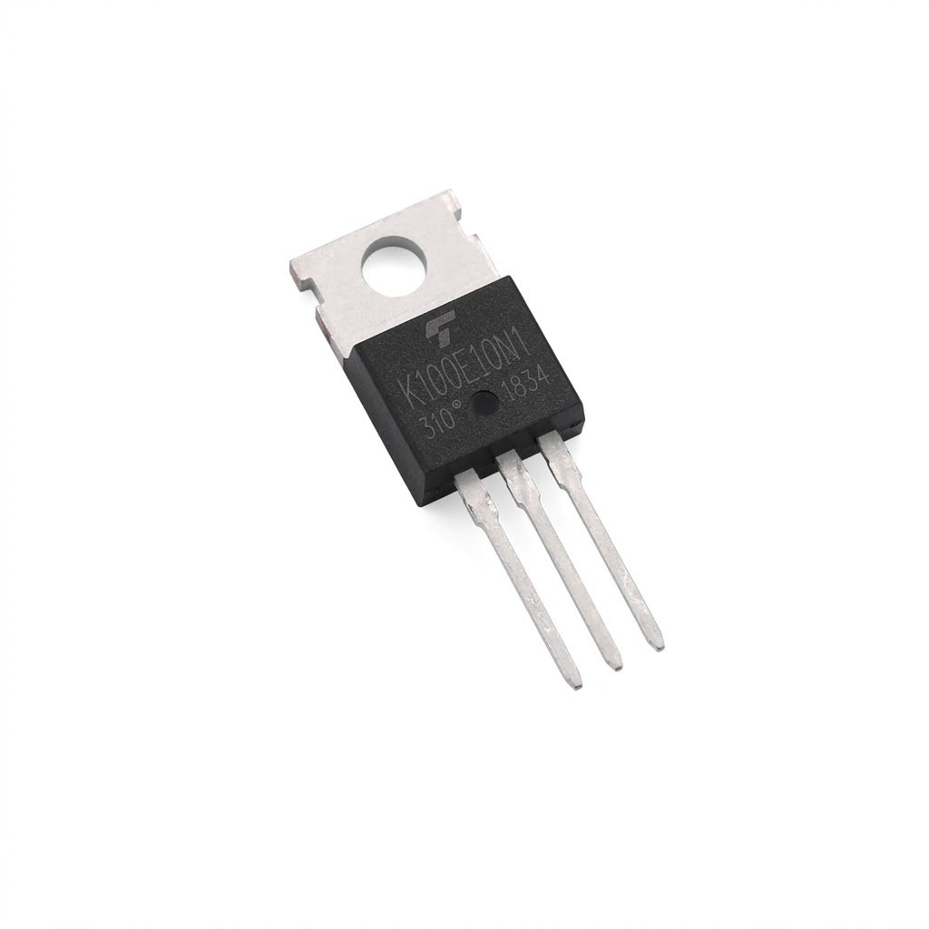
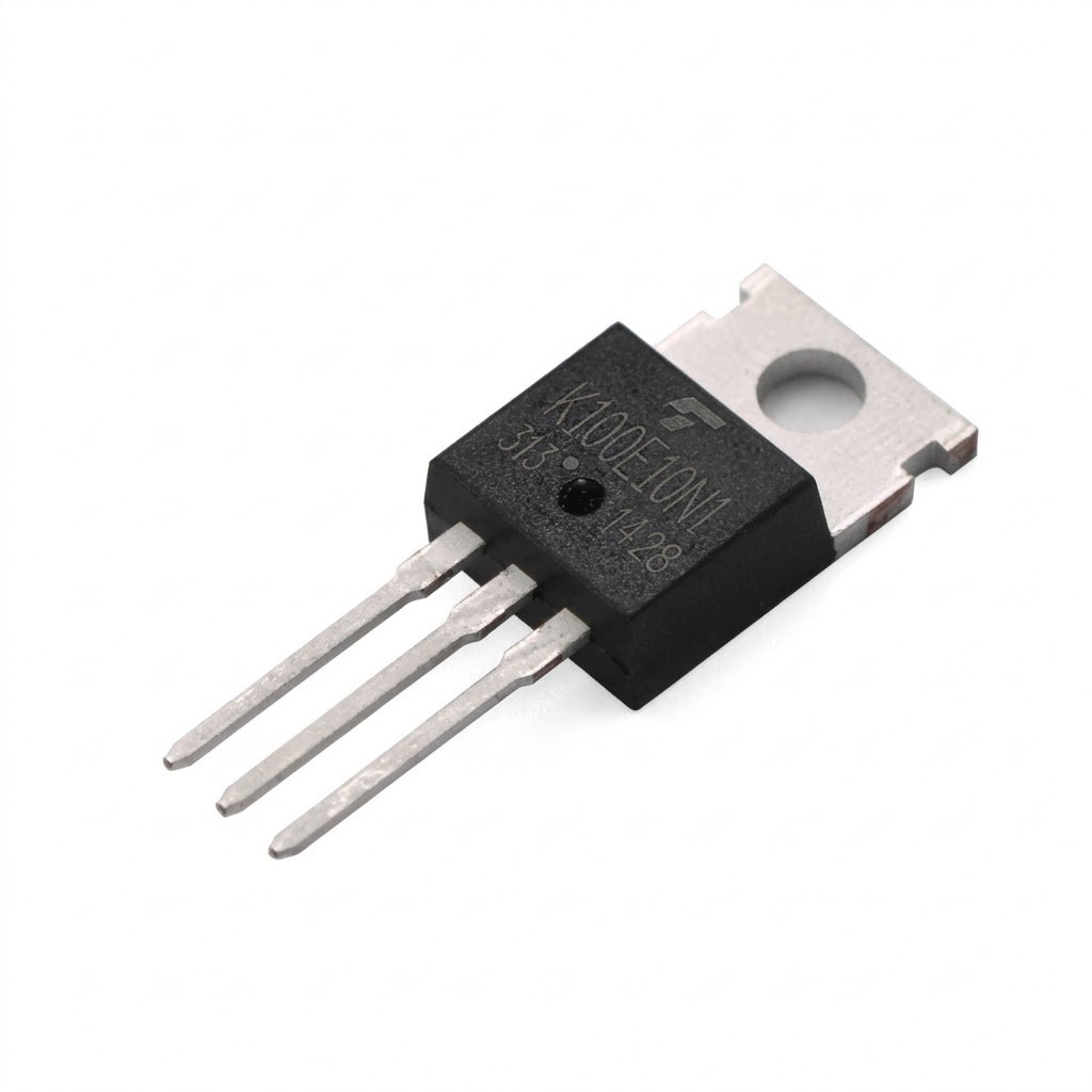
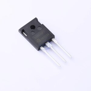
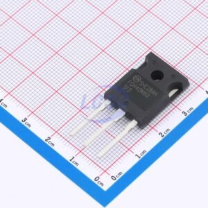
The Toshiba TK100E10N1 is a single N-channel enhancement mode power MOSFET manufactured using Toshiba’s U-MOSⅧ-H process, housed in a standard TO-220 through-hole package. This device features extremely low on-resistance (typical value 2.8mΩ, maximum 3.4mΩ) and high current handling capability (continuous drain current up to 207A), making it very suitable for switching voltage regulators, synchronous rectification, DC-DC converters, and other high-efficiency power conversion circuits.
₨220.00 ₨230.00
Out of stock
The Toshiba TK100E10N1 is a single N-channel enhancement mode power MOSFET manufactured using Toshiba’s U-MOSⅧ-H process, housed in a standard TO-220 through-hole package. This device features extremely low on-resistance (typical value 2.8mΩ, maximum 3.4mΩ) and high current handling capability (continuous drain current up to 207A), making it very suitable for switching voltage regulators, synchronous rectification, DC-DC converters, and other high-efficiency power conversion circuits.
Key Parameters (Absolute Maximum Ratings)
| Parameter | Symbol | Value | Unit |
|---|---|---|---|
| Drain-Source Voltage | VDSS | 100 | V |
| Gate-Source Voltage | VGSS | ±20 | V |
| Continuous Drain Current | ID | 207 | A |
| Power Dissipation | PD | 255 | W |
Electrical Characteristics (Typical/Maximum Values)
| Parameter | Symbol | Test Condition | Value |
|---|---|---|---|
| Drain-Source On-Resistance | RDS(ON) | VGS=10V | Max 3.4 mΩ |
| Gate Threshold Voltage | Vth | – | 2.0 ~ 4.0 V |
| Total Gate Charge | Qg | VGS=10V | Typ 140 nC |
| Input Capacitance | Ciss | – | Typ 8800 pF |
| Reverse Recovery Time | trr | – | Typ 93 ns |
Package Information
-
Package Type: TO-220 (3-pin, through-hole)
-
Dimensions (W×L×H): 10.16 × 15.1 × 4.45 mm
-
Mounting Type: Through-hole (Through Hole)
-
RoHS: Compliant
Main Features/Application Scenarios
-
Low On-Resistance: RDS(ON) typically only 2.8mΩ, reducing conduction losses.
-
High Current Capability: 207A continuous drain current, suitable for high-power density designs.
-
Fast Switching: Low gate charge (140nC) and short reverse recovery time, beneficial for improving switching frequency and efficiency.
-
Typical Applications: Switching voltage regulators, DC-DC converters, synchronous rectification, motor drive, inverter power supplies, etc..
There are no reviews yet.